Essay
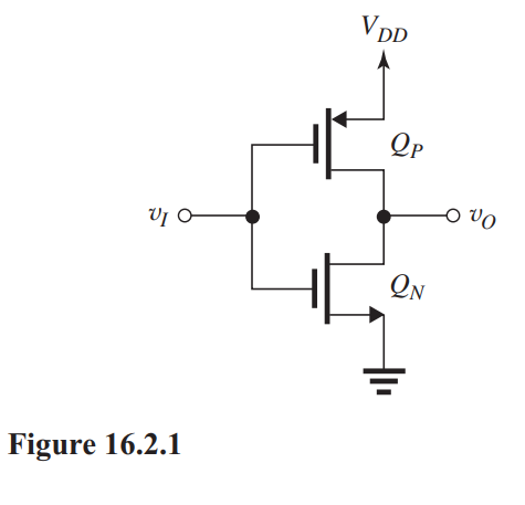
The CMOS inverter shown in Fig. 16.2.1 has and is fabricated in a process for which , and . For this problem, neglect the Early effect. Both and use the minimum channel length allowed. For .
(a) Find the dimensions that must have in order for the inverter switching to occur at .
(b) What are the noise margins of the inverter?
(c) What current flows in and at the switching point?
(d) For , what is the maximum current that can sink while is limited to ?
Correct Answer:
Verified
Figure 16.2.1
(a) For the inverter sw...
View Answer
Unlock this answer now
Get Access to more Verified Answers free of charge
Related Questions