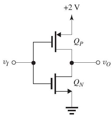
Solved

Figure 161 QNQ_{N} And QPQ_{P} Have Vt=0.5 V\left|V_{t}\right|=0.5 \mathrm{~V} And kn=kp=1 mA/V2k_{n}=k_{p}=1 \mathrm{~mA} / \mathrm{V}^{2} Sketch and Clearly Label the VTC

Question 6

Essay

     Figure 16.1.1 (a) For the CMOS inverter in Fig. 16.1.1,  Q_{N}  and  Q_{P}  have  \left|V_{t}\right|=0.5 \mathrm{~V}  and  k_{n}=k_{p}=1 \mathrm{~mA} / \mathrm{V}^{2} . Sketch and clearly label the VTC  v_{O}  versus  v_{I}  and give values for the noise margins  N M_{L}  and  N M_{H} . What is the output resistance when  v_{O}=0 \mathrm{~V}  ? (b) Provide the CMOS realization of the logic function.  Y=\overline{A(B+C)+D}

Figure 16.1.1
(a) For the CMOS inverter in Fig. 16.1.1, QNQ_{N} and QPQ_{P} have Vt=0.5 V\left|V_{t}\right|=0.5 \mathrm{~V} and kn=kp=1 mA/V2k_{n}=k_{p}=1 \mathrm{~mA} / \mathrm{V}^{2} . Sketch and clearly label the VTC vOv_{O} versus vIv_{I} and give values for the noise margins NMLN M_{L} and NMHN M_{H} . What is the output resistance when vO=0 Vv_{O}=0 \mathrm{~V} ?
(b) Provide the CMOS realization of the logic function.
Y=A(B+C)+DY=\overline{A(B+C)+D}

Correct Answer:

verifed

Verified

blured image

(a) The VTC is shown in Fig. 16.1.2.
...

View Answer

Unlock this answer now
Get Access to more Verified Answers free of charge

Related Questions

Unlock this Answer For Free Now!

View this answer and more for free by performing one of the following actions

qr-code

Scan the QR code to install the App and get 2 free unlocks

upload documents

Unlock quizzes for free by uploading documents