The biasing configuration shown in Figure 7-18 is derived from emitter bias and is referred to as 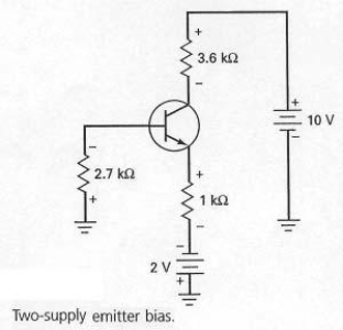
A) emitter derived bias (EDB) .
B) bi-polar emitter bias (BPEB) .
C) two-supply emitter bias (TSEB) .
D) one-supply emitter bias (OSEB) .
Correct Answer:
Verified
Q30: Using a firm voltage divider means that
Q31: The most widely used transistor biasing circuit
Q32: Emitter-feedback and collector-feedback bias circuits are inadequate
Q33: Emitter-feedback bias has never become popular because
Q34: In Figure 7-5,if the fuse blows open
Q36: In Figure 7-5,when the fuse is not
Q37: The main advantage of an optocoupler is
A)
Q38: Voltage-divider bias produces a fixed value of
Q39: With a pnp transistor,the base-emitter junction will
Q40: Collector-feedback bias is more effective than emitter-feedback
Unlock this Answer For Free Now!
View this answer and more for free by performing one of the following actions

Scan the QR code to install the App and get 2 free unlocks

Unlock quizzes for free by uploading documents