Essay
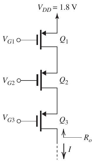
Figure 8.3.1
Design the double-cascode current source shown in Fig. 8.3.1 to provide and the largest possible signal swing at the output; that is, design for the minimum allowable voltage across each transistor. The CMOS fabrication process available has , and . Use devices with , and operate at .
(a) Specify , and .
(b) Find the ratios of the transistors.
(c) What is the value of achieved?
(d) What is the maximum allowable voltage at the current-source output?
(e) If this current source is used as the load of an NMOS double-cascode amplifier having a shortcircuit transconductance of and an output resistance equal to of the current source, what voltage gain is obtained?
Correct Answer:
Verified
Related Questions