Deck 5: Transistor Bias Circuits
Full screen (f)
Question
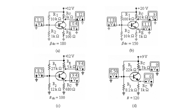
Refer to a)in the figure above. The most probable cause of trouble, if any, from these voltage measurements would be
A)RE is open.
B)the base- emitter junction is open.
C)a short from collector to emitter.
D)There are no problems.
Question
Question
Question
Question
Question
Question

Refer to the figure above. If the transistor were replaced with a transistor whose fidc = 200, the change that might occur is
A)VC would change a small amount.
B)VC would increase to near 20 V.
C)IB would increase significantly.
D)VC would decrease to near 0 V.
Question
Question

Refer to the figure above. If fiDC = 100, the minimum value of IB that would cause this transistor to saturate is
A)1 mA.
B)100 µA.
C)0.1 mA.
D)50 µA.
Question
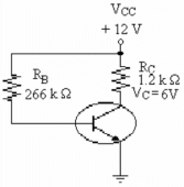
Refer to the figure above. The voltage at the base of this silicon transistor is
A)0.3 V.
B)12 V.
C)0 V.
D)11.3 V.
E)0.7 V.
Question
Question
Question
Question
Question
Question
Question
Question

Refer to d)in the figure above. The most probable cause of trouble, if any, from these voltage measurements is
A)a short from collector to emitter.
B)RE is open.
C)the base- emitter junction is open.
D)There are no problems.
Question
Refer to c)in the figure above. The most probable cause of trouble, if any, from these voltage measurements is
A)the base- emitter junction is open.
B)a short from collector to emitter.
C)RE is open.
D)There are no problems.
Question
Question
Question
Question
Question

Refer to the figure above. The value of RC that will produce a value of VC = 10 V is
A)500 ▲.
B)1 k▲.
C)2.2 k▲.
D)2 k▲.
Question

Refer to the figure above. The purpose of RC is to
A)maintain VBE at 0.7 V.
B)stabilize the operating point with negative feedback.
C)develop the output voltage.
D)establish a dc base voltage.
Question
Question

Refer to b)in the figure above. The most probable cause of trouble, if any, from these voltage measurements is
A)a short from collector to emitter.
B)RE is open.
C)the base- emitter junction is open.
D)There are no problems.
Question
Question
Question
Question
Refer to the figure above. The purpose for R1 and R2 is to
A)maintain VBE at 0.7 V.
B)stabilize the operating point with negative feedback.
C)develop the output voltage.
D)establish a dc base voltage.
Question
Question

Unlock Deck
Sign up to unlock the cards in this deck!
Unlock Deck
Unlock Deck
1/33
Play
Full screen (f)
Deck 5: Transistor Bias Circuits
1
Refer to a)in the figure above. The most probable cause of trouble, if any, from these voltage measurements would be
A)RE is open.
B)the base- emitter junction is open.
C)a short from collector to emitter.
D)There are no problems.
A
2
The most suitable biasing technique used is the
A)base- bias.
B)collector- bias.
C)emitter- bias.
D)voltage- divider bias.
A)base- bias.
B)collector- bias.
C)emitter- bias.
D)voltage- divider bias.
D
3
For linear operation, it is usual to set the Q- point so that
A)VCE = VCC.
B)VCE = VCC/2.
C)VCE = VE.
D)VCE = VCC/4.
A)VCE = VCC.
B)VCE = VCC/2.
C)VCE = VE.
D)VCE = VCC/4.
B
4
A certain transistor in a fixed- bias circuit has the following values: IB = 50 µA, fiDC = 125, VCC = 18 V, and RC = 1.2 k▲. VC is
A)10.5 V.
B)18 V.
C)0 V.
D)7.5 V.
A)10.5 V.
B)18 V.
C)0 V.
D)7.5 V.
Unlock Deck
Unlock for access to all 33 flashcards in this deck.
Unlock Deck
k this deck
5
Base bias provides
A)a very unstable Q- point.
B)zero current in the base and collector circuits.
C)no current gain.
D)a very stable Q- point.
A)a very unstable Q- point.
B)zero current in the base and collector circuits.
C)no current gain.
D)a very stable Q- point.
Unlock Deck
Unlock for access to all 33 flashcards in this deck.
Unlock Deck
k this deck
6
A linear amplifier should have the Q- point located
A)in the distortion region.
B)close to saturation.
C)approximately half- way between saturation and cutoff.
D)close to cutoff.
A)in the distortion region.
B)close to saturation.
C)approximately half- way between saturation and cutoff.
D)close to cutoff.
Unlock Deck
Unlock for access to all 33 flashcards in this deck.
Unlock Deck
k this deck
7
Refer to the figure above. If the transistor were replaced with a transistor whose fidc = 200, the change that might occur is
A)VC would change a small amount.
B)VC would increase to near 20 V.
C)IB would increase significantly.
D)VC would decrease to near 0 V.
Unlock Deck
Unlock for access to all 33 flashcards in this deck.
Unlock Deck
k this deck
8
If a transistor operates at the middle of the dc load line, a decrease in the current gain will move the Q- point
A)off the load line.
B)down.
C)up.
D)nowhere.
A)off the load line.
B)down.
C)up.
D)nowhere.
Unlock Deck
Unlock for access to all 33 flashcards in this deck.
Unlock Deck
k this deck
9
Refer to the figure above. If fiDC = 100, the minimum value of IB that would cause this transistor to saturate is
A)1 mA.
B)100 µA.
C)0.1 mA.
D)50 µA.
Unlock Deck
Unlock for access to all 33 flashcards in this deck.
Unlock Deck
k this deck
10
Refer to the figure above. The voltage at the base of this silicon transistor is
A)0.3 V.
B)12 V.
C)0 V.
D)11.3 V.
E)0.7 V.
Unlock Deck
Unlock for access to all 33 flashcards in this deck.
Unlock Deck
k this deck
11
If the base- emitter junction opens in a voltage- divider biased circuit, the emitter voltage will measure
A)0.7 V less than the base.
B)a voltage nearly equal to VCC.
C)0.7 V more than the base.
D)0 V.
A)0.7 V less than the base.
B)a voltage nearly equal to VCC.
C)0.7 V more than the base.
D)0 V.
Unlock Deck
Unlock for access to all 33 flashcards in this deck.
Unlock Deck
k this deck
12
Saturation and cutoff are operating conditions that are very useful when operating the transistor as
A)a current amplifier.
B)a linear amplifier.
C)a switch.
D)None of the above.
A)a current amplifier.
B)a linear amplifier.
C)a switch.
D)None of the above.
Unlock Deck
Unlock for access to all 33 flashcards in this deck.
Unlock Deck
k this deck
13
A circuit with a fixed emitter current is called
A)one- supply bias.
B)base- bias.
C)emitter- bias.
D)grid- bias.
A)one- supply bias.
B)base- bias.
C)emitter- bias.
D)grid- bias.
Unlock Deck
Unlock for access to all 33 flashcards in this deck.
Unlock Deck
k this deck
14
Adding an emitter resistor to a base- bias circuit produces a bias circuit called
A)base- emitter bias.
B)emitter- feedback bias.
C)emitter bias.
D)None of the above.
A)base- emitter bias.
B)emitter- feedback bias.
C)emitter bias.
D)None of the above.
Unlock Deck
Unlock for access to all 33 flashcards in this deck.
Unlock Deck
k this deck
15
Improper biasing can cause distortion in an amplifier's
A)output signal.
B)input signal.
C)frequency response.
D)power dissipation.
A)output signal.
B)input signal.
C)frequency response.
D)power dissipation.
Unlock Deck
Unlock for access to all 33 flashcards in this deck.
Unlock Deck
k this deck
16
The first step in analyzing emitter- biased circuits is to find the
A)base current.
B)collector current.
C)transistor power.
D)emitter voltage.
A)base current.
B)collector current.
C)transistor power.
D)emitter voltage.
Unlock Deck
Unlock for access to all 33 flashcards in this deck.
Unlock Deck
k this deck
17
Voltage- divider bias provides
A)an unstable Q- point.
B)a Q- point that easily varies with changes in the transistor's current gain.
C)a stable Q- point.
D)Both A and C above.
A)an unstable Q- point.
B)a Q- point that easily varies with changes in the transistor's current gain.
C)a stable Q- point.
D)Both A and C above.
Unlock Deck
Unlock for access to all 33 flashcards in this deck.
Unlock Deck
k this deck
18
Refer to d)in the figure above. The most probable cause of trouble, if any, from these voltage measurements is
A)a short from collector to emitter.
B)RE is open.
C)the base- emitter junction is open.
D)There are no problems.
Unlock Deck
Unlock for access to all 33 flashcards in this deck.
Unlock Deck
k this deck
19
Refer to c)in the figure above. The most probable cause of trouble, if any, from these voltage measurements is
A)the base- emitter junction is open.
B)a short from collector to emitter.
C)RE is open.
D)There are no problems.
Unlock Deck
Unlock for access to all 33 flashcards in this deck.
Unlock Deck
k this deck
20
Three different Q- points are shown on a dc load line. The upper Q- point represents the
A)cutoff point.
B)maximum current gain.
C)minimum current gain.
D)intermediate current gain.
A)cutoff point.
B)maximum current gain.
C)minimum current gain.
D)intermediate current gain.
Unlock Deck
Unlock for access to all 33 flashcards in this deck.
Unlock Deck
k this deck
21
The emitter resistor in a voltage- divider bias circuit is open. The collector voltage will equal approximately
A)one- half VCC.
B)0 V.
C)VCC.
D)None of the above.
A)one- half VCC.
B)0 V.
C)VCC.
D)None of the above.
Unlock Deck
Unlock for access to all 33 flashcards in this deck.
Unlock Deck
k this deck
22
If the collector resistor decreases to zero in a base- biased circuit, the load line will become
A)useless.
B)horizontal.
C)vertical.
D)flat.
A)useless.
B)horizontal.
C)vertical.
D)flat.
Unlock Deck
Unlock for access to all 33 flashcards in this deck.
Unlock Deck
k this deck
23
An indication of cutoff is that
A)VCE = 0 V.
B)IC = ICsat).
C)VCE = VCC.
D)VBE = 0.7 V.
A)VCE = 0 V.
B)IC = ICsat).
C)VCE = VCC.
D)VBE = 0.7 V.
Unlock Deck
Unlock for access to all 33 flashcards in this deck.
Unlock Deck
k this deck
24
Refer to the figure above. The value of RC that will produce a value of VC = 10 V is
A)500 ▲.
B)1 k▲.
C)2.2 k▲.
D)2 k▲.
Unlock Deck
Unlock for access to all 33 flashcards in this deck.
Unlock Deck
k this deck
25
Refer to the figure above. The purpose of RC is to
A)maintain VBE at 0.7 V.
B)stabilize the operating point with negative feedback.
C)develop the output voltage.
D)establish a dc base voltage.
Unlock Deck
Unlock for access to all 33 flashcards in this deck.
Unlock Deck
k this deck
26
Two important yet easily measured quantities that can help determine if a transistor amplifier is operating correctly are
A)IC and VC.
B)fidc and IB.
C)VC and VBE.
D)VBE and IE.
A)IC and VC.
B)fidc and IB.
C)VC and VBE.
D)VBE and IE.
Unlock Deck
Unlock for access to all 33 flashcards in this deck.
Unlock Deck
k this deck
27
Refer to b)in the figure above. The most probable cause of trouble, if any, from these voltage measurements is
A)a short from collector to emitter.
B)RE is open.
C)the base- emitter junction is open.
D)There are no problems.
Unlock Deck
Unlock for access to all 33 flashcards in this deck.
Unlock Deck
k this deck
28
The main difference between an NPN and PNP transistor amplifier is that
A)PNP transistors cannot amplify sine waves.
B)PNP transistors require opposite bias polarities as compared to NPN.
C)PNP transistors need more heat sinking.
D)NPN transistors are linear amplifiers, while PNP amplifiers are nonlinear.
A)PNP transistors cannot amplify sine waves.
B)PNP transistors require opposite bias polarities as compared to NPN.
C)PNP transistors need more heat sinking.
D)NPN transistors are linear amplifiers, while PNP amplifiers are nonlinear.
Unlock Deck
Unlock for access to all 33 flashcards in this deck.
Unlock Deck
k this deck
29
The Q- point of a two supply emitter- bias circuit is not affected by
A)current gain.
B)emitter resistance.
C)collector resistance.
D)VCC.
A)current gain.
B)emitter resistance.
C)collector resistance.
D)VCC.
Unlock Deck
Unlock for access to all 33 flashcards in this deck.
Unlock Deck
k this deck
30
On a dc load line, the area between saturation and cutoff is called the
A)saturation zone.
B)linear region.
C)depletion region.
D)breakdown region.
A)saturation zone.
B)linear region.
C)depletion region.
D)breakdown region.
Unlock Deck
Unlock for access to all 33 flashcards in this deck.
Unlock Deck
k this deck
31
Refer to the figure above. The purpose for R1 and R2 is to
A)maintain VBE at 0.7 V.
B)stabilize the operating point with negative feedback.
C)develop the output voltage.
D)establish a dc base voltage.
Unlock Deck
Unlock for access to all 33 flashcards in this deck.
Unlock Deck
k this deck
32
For transistors using voltage- divider bias, the base current should be
A)much larger than the current through the voltage divider.
B)Beta times larger than the collector current.
C)about one- half the collector current.
D)much smaller than the current through the voltage divider.
A)much larger than the current through the voltage divider.
B)Beta times larger than the collector current.
C)about one- half the collector current.
D)much smaller than the current through the voltage divider.
Unlock Deck
Unlock for access to all 33 flashcards in this deck.
Unlock Deck
k this deck
33
For a properly designed emitter- bias circuit, changes in current gain
A)affect the collector voltage.
B)severely affect the Q- point.
C)do not occur in the transistor.
D)do not affect the Q- point.
A)affect the collector voltage.
B)severely affect the Q- point.
C)do not occur in the transistor.
D)do not affect the Q- point.
Unlock Deck
Unlock for access to all 33 flashcards in this deck.
Unlock Deck
k this deck
Unlock Deck
Unlock for access to all 33 flashcards in this deck.