Deck 9: Fet Amplifiers and Switching Circuits
Full screen (f)
Question
Question

Refer to the figure above. If ID = 6 mA, the value of VGS is
A)- 19.8 V.
B)- 10.2 V.
C)9 V.
D)- 9 V.
Question
A CS amplifier has a voltage gain of 
Question
Question

Refer to the figure above. If R3 opened, Vout would
A)increase.
B)decrease.
C)remain the same.
D)distort.
Question
Refer to the figure above. If C5 opened, the signal voltage across R7 would
A)increase.
B)be zero.
C)remain the same.
D)distort.
Question
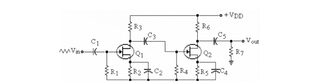
Refer to the figure above. If R7 were to increase in value, Vout would
A)increase.
B)decrease.
C)remain the same.
D)distort.
Question
Question
Question
Question
Refer to the figure above. If R1 opened, Vout would
A)increase.
B)decrease.
C)remain the same.
D)distort.
Question
Question
Question
Question
Question
Question
Question
Question
Question
Question

Refer to the figure above. If C2 opened, Vout would
A)increase.
B)decrease.
C)remain the same.
D)distort.
Question
Question
Question

Refer to the figure above. If C3 opened, Vout would
A)increase.
B)decrease.
C)remain the same.
D)distort.
Question
Question
Refer to the figure above. If the measured value of Vout were below normal, the problem might be that
A)C2 is shorted.
B)RD is open.
C)Vin has increased.
D)C2 is open.
Question

Refer to the figure above. If AV1 = 18 and AVt = 288, the value of AV2 would be
A)16.
B)18.
C)49.18.
D)5184.
Question
Question

Refer to the figure above. If gm = 4000 µS and a signal of 75 mV rms is applied to the gate, the p- p output voltage is
A)1.13 Vp- p.
B)990 Vp- p.
C)2.8 Vp- p.
D)990 mV.
Question
Question
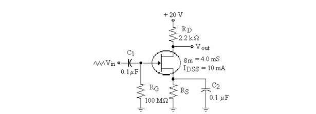
Refer to the figure above. If Vin = 50 mVp- p, the output voltage is
A)4.4 Vp- p.
B)50 mVp- p.
C)0.044 Vp- p.
D)440 mVp- p.
Question
Question
Refer to the figure above. If the source- drain of Q2 shorted, the output signal from Q1 would
A)increase.
B)decrease.
C)remain the same.
D)distort.
Question
Question
Question
Question
Question
Refer to the figure above. If gm = 6500 µS and an input signal of 125 mVp- p is applied to the gate, the output voltage Vout is
A)2.68 Vp- p.
B)1.625 Vp- p.
C)0.8125 Vp- p.
D)6.25 Vp- p.
Question
Refer to the figure above. If R5 opened, Vout would
A)increase.
B)decrease.
C)remain the same.
D)distort.
Question
Refer to the figure above. If Vin = 1 Vp- p, the output voltage Vout would be
A)0 V.
B)undistorted.
C)clipped on the positive peaks.
D)clipped on the negative peaks.

Unlock Deck
Sign up to unlock the cards in this deck!
Unlock Deck
Unlock Deck
1/40
Play
Full screen (f)
Deck 9: Fet Amplifiers and Switching Circuits
1
In a self- biased common- source amplifier, what purpose does resistor RG serve?
A)Keeps the gate at approximately zero volts
B)Develops the gate- source bias current
C)Prevents loading of the ac signal source
D)Both A and C above.
A)Keeps the gate at approximately zero volts
B)Develops the gate- source bias current
C)Prevents loading of the ac signal source
D)Both A and C above.
D
2
Refer to the figure above. If ID = 6 mA, the value of VGS is
A)- 19.8 V.
B)- 10.2 V.
C)9 V.
D)- 9 V.
D
3
A CS amplifier has a voltage gain of
A
4
The ac equivalent circuit of a FET amplifier assumes that the capacitors
A)have an XC of 600 ▲ at the signal frequency.
B)are treated like opens.
C)have an XC of 1 M▲ at the signal frequency.
D)are treated like shorts.
A)have an XC of 600 ▲ at the signal frequency.
B)are treated like opens.
C)have an XC of 1 M▲ at the signal frequency.
D)are treated like shorts.
Unlock Deck
Unlock for access to all 40 flashcards in this deck.
Unlock Deck
k this deck
5
Refer to the figure above. If R3 opened, Vout would
A)increase.
B)decrease.
C)remain the same.
D)distort.
Unlock Deck
Unlock for access to all 40 flashcards in this deck.
Unlock Deck
k this deck
6
Refer to the figure above. If C5 opened, the signal voltage across R7 would
A)increase.
B)be zero.
C)remain the same.
D)distort.
Unlock Deck
Unlock for access to all 40 flashcards in this deck.
Unlock Deck
k this deck
7
Refer to the figure above. If R7 were to increase in value, Vout would
A)increase.
B)decrease.
C)remain the same.
D)distort.
Unlock Deck
Unlock for access to all 40 flashcards in this deck.
Unlock Deck
k this deck
8
Two FET amplifiers operated in cascade have gains of 6 dB and 8 dB. The total overall gain in dB is
A)64 dB.
B)14 dB.
C)2 dB.
D)48 dB.
A)64 dB.
B)14 dB.
C)2 dB.
D)48 dB.
Unlock Deck
Unlock for access to all 40 flashcards in this deck.
Unlock Deck
k this deck
9
Which of the following is not a FET amplifier?
A)Emitter- follower
B)Common- drain
C)Source- follower
D)Common- gate
A)Emitter- follower
B)Common- drain
C)Source- follower
D)Common- gate
Unlock Deck
Unlock for access to all 40 flashcards in this deck.
Unlock Deck
k this deck
10
If the interstage coupling capacitor opens in a two stage FET amplifier, the output signal will
A)double in amplitude.
B)be slightly increased.
C)be slightly decreased.
D)be zero.
A)double in amplitude.
B)be slightly increased.
C)be slightly decreased.
D)be zero.
Unlock Deck
Unlock for access to all 40 flashcards in this deck.
Unlock Deck
k this deck
11
Refer to the figure above. If R1 opened, Vout would
A)increase.
B)decrease.
C)remain the same.
D)distort.
Unlock Deck
Unlock for access to all 40 flashcards in this deck.
Unlock Deck
k this deck
12
The capacitor connected to the source of a common source amplifier
A)is used for input coupling.
B)makes the source an ac ground point.
C)is needed for extra power supply filtering.
D)is used for output coupling.
A)is used for input coupling.
B)makes the source an ac ground point.
C)is needed for extra power supply filtering.
D)is used for output coupling.
Unlock Deck
Unlock for access to all 40 flashcards in this deck.
Unlock Deck
k this deck
13
The main reason that the input resistance of FET amplifiers is so high is that the
A)gate junction is reverse- biased.
B)power supplies used are high voltage/low current.
C)biasing resistors are extremely small.
D)FET junctions are forward- biased and made of germanium.
A)gate junction is reverse- biased.
B)power supplies used are high voltage/low current.
C)biasing resistors are extremely small.
D)FET junctions are forward- biased and made of germanium.
Unlock Deck
Unlock for access to all 40 flashcards in this deck.
Unlock Deck
k this deck
14
Which of the following is not an application of an analog MOSFET switch?
A)Switched capacitor circuit
B)Sample- and- hold circuit
C)Inverter
D)Analog multiplexer
A)Switched capacitor circuit
B)Sample- and- hold circuit
C)Inverter
D)Analog multiplexer
Unlock Deck
Unlock for access to all 40 flashcards in this deck.
Unlock Deck
k this deck
15
Refer to the figure above. Assuming midpoint biasing, if VGS = - 4 V, the value of RS that will provide this value is
A)1.2 k▲.
B)800 ▲.
C)80 ▲.
D)600 ▲.
A)1.2 k▲.
B)800 ▲.
C)80 ▲.
D)600 ▲.
Unlock Deck
Unlock for access to all 40 flashcards in this deck.
Unlock Deck
k this deck
16
Which of the following is not a characteristic of a JFET- based cascode amplifier?
A)High input resistance
B)High frequency response
C)High gain
D)High input capacitance
A)High input resistance
B)High frequency response
C)High gain
D)High input capacitance
Unlock Deck
Unlock for access to all 40 flashcards in this deck.
Unlock Deck
k this deck
17
When the input signal is large, a source follower has
A)a small distortion.
B)a voltage gain of less than one.
C)a high input resistance.
D)All of the above.
A)a small distortion.
B)a voltage gain of less than one.
C)a high input resistance.
D)All of the above.
Unlock Deck
Unlock for access to all 40 flashcards in this deck.
Unlock Deck
k this deck
18
Refer to the figure above. If ID = 4 mA, IDSS = 16 mA, and VGSoff)= - 8 V, VDS would be
A)10.8 V.
B)19.2 V.
C)30 V.
D)- 6 V.
A)10.8 V.
B)19.2 V.
C)30 V.
D)- 6 V.
Unlock Deck
Unlock for access to all 40 flashcards in this deck.
Unlock Deck
k this deck
19
Changing can control the voltage gain of a common- source amplifier.
A)VDD
B)gm
C)RS
D)the input voltage
A)VDD
B)gm
C)RS
D)the input voltage
Unlock Deck
Unlock for access to all 40 flashcards in this deck.
Unlock Deck
k this deck
20
Which of the following is not part of a class D amplifier?
A)Switching amplifier
B)Low- pass filter
C)Oscillator
D)Pulse- width modulator
A)Switching amplifier
B)Low- pass filter
C)Oscillator
D)Pulse- width modulator
Unlock Deck
Unlock for access to all 40 flashcards in this deck.
Unlock Deck
k this deck
21
Refer to the figure above. If C2 opened, Vout would
A)increase.
B)decrease.
C)remain the same.
D)distort.
Unlock Deck
Unlock for access to all 40 flashcards in this deck.
Unlock Deck
k this deck
22
Refer to the figure above. If C2 opened, the output signal would
A)decrease and then increase.
B)increase in value.
C)not change.
D)decrease in value.
A)decrease and then increase.
B)increase in value.
C)not change.
D)decrease in value.
Unlock Deck
Unlock for access to all 40 flashcards in this deck.
Unlock Deck
k this deck
23
If RS is not bypassed,
A)the dc power supply will have excessive ripple.
B)the gain will be extremely high.
C)no signal will be coupled to the output.
D)the gain will be reduced.
A)the dc power supply will have excessive ripple.
B)the gain will be extremely high.
C)no signal will be coupled to the output.
D)the gain will be reduced.
Unlock Deck
Unlock for access to all 40 flashcards in this deck.
Unlock Deck
k this deck
24
Refer to the figure above. If C3 opened, Vout would
A)increase.
B)decrease.
C)remain the same.
D)distort.
Unlock Deck
Unlock for access to all 40 flashcards in this deck.
Unlock Deck
k this deck
25
Two FET amplifiers are operated in cascade. If the gain of the amplifiers is equal and the total overall gain is 25, the gain of each amplifier is
A)12.5.
B)5.
C)2.
D)7.25.
A)12.5.
B)5.
C)2.
D)7.25.
Unlock Deck
Unlock for access to all 40 flashcards in this deck.
Unlock Deck
k this deck
26
Refer to the figure above. If the measured value of Vout were below normal, the problem might be that
A)C2 is shorted.
B)RD is open.
C)Vin has increased.
D)C2 is open.
Unlock Deck
Unlock for access to all 40 flashcards in this deck.
Unlock Deck
k this deck
27
Refer to the figure above. If AV1 = 18 and AVt = 288, the value of AV2 would be
A)16.
B)18.
C)49.18.
D)5184.
Unlock Deck
Unlock for access to all 40 flashcards in this deck.
Unlock Deck
k this deck
28
A common- source amplifier has a phase shift between the input and the output.
A)360°
B)180°
C)45°
D)90°
A)360°
B)180°
C)45°
D)90°
Unlock Deck
Unlock for access to all 40 flashcards in this deck.
Unlock Deck
k this deck
29
Refer to the figure above. If gm = 4000 µS and a signal of 75 mV rms is applied to the gate, the p- p output voltage is
A)1.13 Vp- p.
B)990 Vp- p.
C)2.8 Vp- p.
D)990 mV.
Unlock Deck
Unlock for access to all 40 flashcards in this deck.
Unlock Deck
k this deck
30
Where is the input signal applied in a common- gate amplifier?
A)Gate
B)Drain
C)Source
D)Base
A)Gate
B)Drain
C)Source
D)Base
Unlock Deck
Unlock for access to all 40 flashcards in this deck.
Unlock Deck
k this deck
31
Refer to the figure above. If Vin = 50 mVp- p, the output voltage is
A)4.4 Vp- p.
B)50 mVp- p.
C)0.044 Vp- p.
D)440 mVp- p.
Unlock Deck
Unlock for access to all 40 flashcards in this deck.
Unlock Deck
k this deck
32
Refer to the figure above. If C4 opened, the signal voltage at the drain of Q1 would
A)increase.
B)decrease.
C)remain the same.
D)distort.
A)increase.
B)decrease.
C)remain the same.
D)distort.
Unlock Deck
Unlock for access to all 40 flashcards in this deck.
Unlock Deck
k this deck
33
Refer to the figure above. If the source- drain of Q2 shorted, the output signal from Q1 would
A)increase.
B)decrease.
C)remain the same.
D)distort.
Unlock Deck
Unlock for access to all 40 flashcards in this deck.
Unlock Deck
k this deck
34
When troubleshooting a multiple stage CS amplifier, signal tracing reveals a significant amount of signal voltage at the source of the first stage. The most likely problem is
A)an open coupling capacitor from signal source.
B)too much dc supply voltage.
C)a shorted load in third stage.
D)an open source bypass capacitor.
A)an open coupling capacitor from signal source.
B)too much dc supply voltage.
C)a shorted load in third stage.
D)an open source bypass capacitor.
Unlock Deck
Unlock for access to all 40 flashcards in this deck.
Unlock Deck
k this deck
35
Two common- source amplifiers are cascaded. The overall phase shift from the input of the first amplifier to the output of the second amplifier is
A)45°.
B)90°.
C)0°.
D)180°.
A)45°.
B)90°.
C)0°.
D)180°.
Unlock Deck
Unlock for access to all 40 flashcards in this deck.
Unlock Deck
k this deck
36
What is the role of the low- pass filter in a class D amplifier?
A)Remove hum
B)Prevent oscillation
C)Remove the modulating frequency and harmonics
D)Limit amplifier frequency response
A)Remove hum
B)Prevent oscillation
C)Remove the modulating frequency and harmonics
D)Limit amplifier frequency response
Unlock Deck
Unlock for access to all 40 flashcards in this deck.
Unlock Deck
k this deck
37
What component of an FET amplifier needs to be at least ten times greater than RD to ensure maximum voltage gain?
A)gm
B)r'ds
C)Rs
D)RS
A)gm
B)r'ds
C)Rs
D)RS
Unlock Deck
Unlock for access to all 40 flashcards in this deck.
Unlock Deck
k this deck
38
Refer to the figure above. If gm = 6500 µS and an input signal of 125 mVp- p is applied to the gate, the output voltage Vout is
A)2.68 Vp- p.
B)1.625 Vp- p.
C)0.8125 Vp- p.
D)6.25 Vp- p.
Unlock Deck
Unlock for access to all 40 flashcards in this deck.
Unlock Deck
k this deck
39
Refer to the figure above. If R5 opened, Vout would
A)increase.
B)decrease.
C)remain the same.
D)distort.
Unlock Deck
Unlock for access to all 40 flashcards in this deck.
Unlock Deck
k this deck
40
Refer to the figure above. If Vin = 1 Vp- p, the output voltage Vout would be
A)0 V.
B)undistorted.
C)clipped on the positive peaks.
D)clipped on the negative peaks.
Unlock Deck
Unlock for access to all 40 flashcards in this deck.
Unlock Deck
k this deck
Unlock Deck
Unlock for access to all 40 flashcards in this deck.