Deck 1: Fundamental Solid-State Principles
Full screen (f)
Question
Question
Question
Question
Question
Question
Question
Question
Question
Question
Question
Question
Question
Question
Question
Question
Question
Question
Question
Question
Question
Question
Question
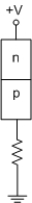
What type of junction bias is shown?
A) Forward bias
B) Reverse bias
C) Zero bias
Question
Question
Question
Question
Question
Question
Question
Question
Question
Question
Question
Question

Unlock Deck
Sign up to unlock the cards in this deck!
Unlock Deck
Unlock Deck
1/35
Play
Full screen (f)
Deck 1: Fundamental Solid-State Principles
1
Gold has one valence electron, tin has four valence electrons, and argon has eight valence electrons. Which of these elements has the highest conductivity?
A) Gold
B) Tin
C) Argon
A) Gold
B) Tin
C) Argon
Gold
2
The difference between the energy levels of two orbital shells is called the
A) conduction gap.
B) energy band.
C) valence band.
D) energy gap.
A) conduction gap.
B) energy band.
C) valence band.
D) energy gap.
energy gap.
3
N-type materials are electrically in their natural state.
A) negative
B) positive
C) neutral
A) negative
B) positive
C) neutral
neutral
4
Doping is used to
A) decrease the conductivity of an intrinsic semiconductor.
B) increase the conductivity of an intrinsic semiconductor.
C) limit the conductivity of an intrinsic semiconductor.
A) decrease the conductivity of an intrinsic semiconductor.
B) increase the conductivity of an intrinsic semiconductor.
C) limit the conductivity of an intrinsic semiconductor.
Unlock Deck
Unlock for access to all 35 flashcards in this deck.
Unlock Deck
k this deck
5
Which of the following statements is true?
A) Electrons cannot continually orbit the nucleus of an atom in the space that exists between orbital shells.
B) There is no specific energy level that is associated with a given orbital shell.
C) If an electron jumps from an orbital shell to one that has a higher energy level, it remains in the higher-energy shell permanently.
Unlock Deck
Unlock for access to all 35 flashcards in this deck.
Unlock Deck
k this deck
6
The time between the forming of an electron-hole pair and recombination is called
A) charge time.
B) recombination time.
C) lifetime.
D) conduction time.
A) charge time.
B) recombination time.
C) lifetime.
D) conduction time.
Unlock Deck
Unlock for access to all 35 flashcards in this deck.
Unlock Deck
k this deck
7
When pentavalent elements are used in doping, the resulting material is called material and has an excess of .
A) n-type; valence-band holes
B) n-type; conduction-band electrons
C) p-type; valence-band holes
D) p-type; conduction-band electrons
A) n-type; valence-band holes
B) n-type; conduction-band electrons
C) p-type; valence-band holes
D) p-type; conduction-band electrons
Unlock Deck
Unlock for access to all 35 flashcards in this deck.
Unlock Deck
k this deck
8
P-type materials are electrically in their natural state.
A) negative
B) positive
C) neutral
A) negative
B) positive
C) neutral
Unlock Deck
Unlock for access to all 35 flashcards in this deck.
Unlock Deck
k this deck
9
Which of the following is not a commonly used semiconductor in electronic applications?
A) Carbon
B) Lead
C) Silicon
D) Germanium
A) Carbon
B) Lead
C) Silicon
D) Germanium
Unlock Deck
Unlock for access to all 35 flashcards in this deck.
Unlock Deck
k this deck
10
A depletion layer acts as a/an
A) insulator.
B) semiconductor.
C) conductor.
A) insulator.
B) semiconductor.
C) conductor.
Unlock Deck
Unlock for access to all 35 flashcards in this deck.
Unlock Deck
k this deck
11
Which of the following is a result of covalent bonding in intrinsic silicon?
A) Atoms are held together.
B) The atoms are electrically stable.
C) The material acts as an insulator.
D) All of the above are results of the bonding.
A) Atoms are held together.
B) The atoms are electrically stable.
C) The material acts as an insulator.
D) All of the above are results of the bonding.
Unlock Deck
Unlock for access to all 35 flashcards in this deck.
Unlock Deck
k this deck
12
When trivalent elements are used in doping, the resulting material is called material and has an excess of .
A) n-type; valence-band holes
B) n-type; conduction-band electrons
C) p-type; valence-band holes
D) p-type; conduction-band electrons
A) n-type; valence-band holes
B) n-type; conduction-band electrons
C) p-type; valence-band holes
D) p-type; conduction-band electrons
Unlock Deck
Unlock for access to all 35 flashcards in this deck.
Unlock Deck
k this deck
13
As a result of covalent bonding, intrinsic silicon effectively acts as a/an
A) insulator.
B) semiconductor.
C) conductor.
A) insulator.
B) semiconductor.
C) conductor.
Unlock Deck
Unlock for access to all 35 flashcards in this deck.
Unlock Deck
k this deck
14
The nucleus of an atom contains
A) protons and electrons.
B) neutrons and electrons.
C) neutrons and protons.
D) neutrons, protons, and electrons.
A) protons and electrons.
B) neutrons and electrons.
C) neutrons and protons.
D) neutrons, protons, and electrons.
Unlock Deck
Unlock for access to all 35 flashcards in this deck.
Unlock Deck
k this deck
15
In an n-type material, the majority carriers are
A) conduction-band electrons.
B) conduction-band holes.
C) valence-band electrons.
D) valence-band holes.
E) neutral atoms.
A) conduction-band electrons.
B) conduction-band holes.
C) valence-band electrons.
D) valence-band holes.
E) neutral atoms.
Unlock Deck
Unlock for access to all 35 flashcards in this deck.
Unlock Deck
k this deck
16
Which semiconductor element is most often used in the production of solid state devices?
A) Carbon
B) Lead
C) Silicon
D) Germanium
A) Carbon
B) Lead
C) Silicon
D) Germanium
Unlock Deck
Unlock for access to all 35 flashcards in this deck.
Unlock Deck
k this deck
17
Pentavalent elements have valence electrons).
A) one
B) three
C) five
D) eight
A) one
B) three
C) five
D) eight
Unlock Deck
Unlock for access to all 35 flashcards in this deck.
Unlock Deck
k this deck
18
Trivalent elements have valence electrons).
A) one
B) three
C) five
D) eight
A) one
B) three
C) five
D) eight
Unlock Deck
Unlock for access to all 35 flashcards in this deck.
Unlock Deck
k this deck
19
In a p-type material, the minority carriers are
A) conduction-band electrons.
B) conduction-band holes.
C) valence-band electrons.
D) valence-band holes.
E) charged atoms.
A) conduction-band electrons.
B) conduction-band holes.
C) valence-band electrons.
D) valence-band holes.
E) charged atoms.
Unlock Deck
Unlock for access to all 35 flashcards in this deck.
Unlock Deck
k this deck
20
Conduction through a material with a positive temperature coefficient tends to as temperature increases.
A) increase
B) decrease
C) remain relatively unchanged
A) increase
B) decrease
C) remain relatively unchanged
Unlock Deck
Unlock for access to all 35 flashcards in this deck.
Unlock Deck
k this deck
21
Which of the following is not a trivalent doping element?
A) Aluminum
B) Arsenic
C) Boron
D) Gallium
A) Aluminum
B) Arsenic
C) Boron
D) Gallium
Unlock Deck
Unlock for access to all 35 flashcards in this deck.
Unlock Deck
k this deck
22
Why is silicon more commonly used than germanium in the production of solid-state components?
A) It is cheaper.
B) It is easier to produce.
C) It is more tolerant of heat.
D) All of the above.
A) It is cheaper.
B) It is easier to produce.
C) It is more tolerant of heat.
D) All of the above.
Unlock Deck
Unlock for access to all 35 flashcards in this deck.
Unlock Deck
k this deck
23
What type of junction bias is shown?
A) Forward bias
B) Reverse bias
C) Zero bias
Unlock Deck
Unlock for access to all 35 flashcards in this deck.
Unlock Deck
k this deck
24
A p-type material is joined with an n-type material. When forward biased, the voltage across the junction is approximately 700 mV 0.7 V). The two materials are most likely made of
A) silicon.
B) germanium.
C) carbon.
D) lead.
A) silicon.
B) germanium.
C) carbon.
D) lead.
Unlock Deck
Unlock for access to all 35 flashcards in this deck.
Unlock Deck
k this deck
25
When a pn junction is reverse biased, its resistance is
A) high.
B) low.
C) determined by the components that are external to the device.
A) high.
B) low.
C) determined by the components that are external to the device.
Unlock Deck
Unlock for access to all 35 flashcards in this deck.
Unlock Deck
k this deck
26
When a pn junction is forward biased, the depletion layer is at its width and the device acts as a near-perfect .
A) minimum; conductor
B) minimum; insulator
C) maximum; conductor
D) maximum; insulator
A) minimum; conductor
B) minimum; insulator
C) maximum; conductor
D) maximum; insulator
Unlock Deck
Unlock for access to all 35 flashcards in this deck.
Unlock Deck
k this deck
27
The small amount of current that is present at the forming of a pn junction is called
A) knee current.
B) diffusion current.
C) barrier current.
D) depletion current.
A) knee current.
B) diffusion current.
C) barrier current.
D) depletion current.
Unlock Deck
Unlock for access to all 35 flashcards in this deck.
Unlock Deck
k this deck
28
The simplest model of the atom is called the
A) covalent bond model.
B) conduction bond model.
C) Bohr model.
D) energy gap model.
A) covalent bond model.
B) conduction bond model.
C) Bohr model.
D) energy gap model.
Unlock Deck
Unlock for access to all 35 flashcards in this deck.
Unlock Deck
k this deck
29
The voltage across a forward-biased germanium pn junction is approximately
A) 0.1 V.
B) 0.3 V.
C) 0.7 V.
D) 0.8 V.
A) 0.1 V.
B) 0.3 V.
C) 0.7 V.
D) 0.8 V.
Unlock Deck
Unlock for access to all 35 flashcards in this deck.
Unlock Deck
k this deck
30
Pentavalent atoms are often referred to as
A) donor atoms.
B) minority carriers.
C) acceptor atoms.
D) majority carriers.
A) donor atoms.
B) minority carriers.
C) acceptor atoms.
D) majority carriers.
Unlock Deck
Unlock for access to all 35 flashcards in this deck.
Unlock Deck
k this deck
31
Which of the following is an advantage of transistors over vacuum tubes?
A) Transistors are smaller.
B) Transistors use more power.
C) Transistors are fragile.
D) All of the above
A) Transistors are smaller.
B) Transistors use more power.
C) Transistors are fragile.
D) All of the above
Unlock Deck
Unlock for access to all 35 flashcards in this deck.
Unlock Deck
k this deck
32
When a pn junction is reverse biased, the depletion layer is at its width and the device acts as a near-perfect .
A) minimum; conductor
B) minimum; insulator
C) maximum; conductor
D) maximum; insulator
A) minimum; conductor
B) minimum; insulator
C) maximum; conductor
D) maximum; insulator
Unlock Deck
Unlock for access to all 35 flashcards in this deck.
Unlock Deck
k this deck
33
A pn junction is forward biased when
A) the applied potential causes the n-type material to be more positive than the p-type material.
B) the applied potential causes the n-type material to be more negative than the p-type material.
C) both materials are at the same potential.
D) Both A and C above.
A) the applied potential causes the n-type material to be more positive than the p-type material.
B) the applied potential causes the n-type material to be more negative than the p-type material.
C) both materials are at the same potential.
D) Both A and C above.
Unlock Deck
Unlock for access to all 35 flashcards in this deck.
Unlock Deck
k this deck
34
When a pn junction is forward biased, the combined resistance of the p-type and n-type materials is called
A) net resistance.
B) total resistance.
C) bulk resistance.
D) forward resistance.
A) net resistance.
B) total resistance.
C) bulk resistance.
D) forward resistance.
Unlock Deck
Unlock for access to all 35 flashcards in this deck.
Unlock Deck
k this deck
35
Trivalent atoms are often referred to as
A) donor atoms.
B) minority carriers.
C) acceptor atoms.
D) majority carriers.
A) donor atoms.
B) minority carriers.
C) acceptor atoms.
D) majority carriers.
Unlock Deck
Unlock for access to all 35 flashcards in this deck.
Unlock Deck
k this deck
Unlock Deck
Unlock for access to all 35 flashcards in this deck.