Deck 19: Solid-State Switching Circuits
Full screen (f)
Question
Question
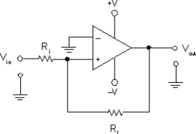
The circuit in Figure has values of Rf= 10 kΩ, Ri= 2 kΩ, and ±10 V supply voltages. What is the LTP voltage for the circuit?
A) 1.8 V
B) 4.5 V
C) -1.8 V
D) -4.5 V
Question
Question
Question
Question
Question
Question
Question
Question
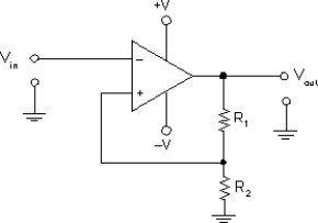
The circuit in Figure has values of R1= 10 kΩ, R2= 20 kΩ, and ±10 V supply voltages. What is the UTP value for the circuit?
A) 6 V
B) -6 V
C) 5.4 V
D) -5.4 V
Question
Question
Question
Question
Question
Question
Question
Question
Question
Question
Question
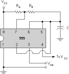
The circuit in Figure has the following values: RA=RB=10 kΩ and C=0.01 μF. What is the operating frequency of the circuit?
A) 7.2 kHz
B) 3.3 kHz
C) 4.8 kHz
D) 3.6 kHz
Question
The 555 timer can be used as a linear amplifier.
Question
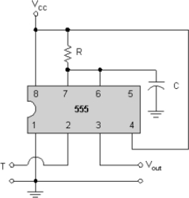
What is the duty cycle of the circuit in Figure ?
A) 66.7%
B) 33%
C) 50%
D) 20%
Question
Question
An engineer needs a circuit that pulses high for 30 ns when it receives an input trigger signal and then returns to its low output state. He should use .
A) a one shot
B) a flip-flop
C) a VCO
D) a CCO
Question
An engineer needs a circuit that oscillates at different frequencies based on the value of a dc input voltage. He should use .
A) a one shot
B) a flip-flop
C) a VCO
D) a CCO
Question
A 555 timer is connected as shown in Figure If the cap on pin #6 is being held at 0 V by pin 7, pin #2 must go below for the output from the timer to go high.
A) +5 V
B) 0 V
C) +3 V
D) +15 V
Question
Question
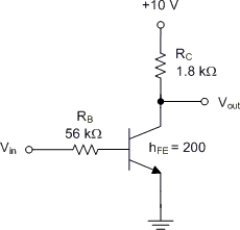
What is the minimum input voltage required to drive the transistor into saturation?
A) 2.15 V
B) 2.26 V
C) 2.66 V
D) 6.3 V
Question
Question
What is the value of ICsat) for the circuit in Figure 19-5?
A) 5.17 mA
B) 5.56 mA
C) 7 mA
D) 10 mA
Question
Which of the following switching circuits would have the lowest power dissipation?
A) BJT
B) JFET
C) MOSFET
D) CMOS
Question
Question
What value of IB is required to drive the transistor into saturation?
A) 25.8 μA
B) 27.8 μA
C) 35 μA
D) 100 μA

Unlock Deck
Sign up to unlock the cards in this deck!
Unlock Deck
Unlock Deck
1/34
Play
Full screen (f)
Deck 19: Solid-State Switching Circuits
1
The output from an inverter has a pulse width of 55 μs and a space width of 30 μs. What is the duty cycle of the circuit?
A) 55%
B) 64.7%
C) 85%
D) 39.3%
A) 55%
B) 64.7%
C) 85%
D) 39.3%
64.7%
2
The circuit in Figure has values of Rf= 10 kΩ, Ri= 2 kΩ, and ±10 V supply voltages. What is the LTP voltage for the circuit?
A) 1.8 V
B) 4.5 V
C) -1.8 V
D) -4.5 V
-1.8 V
3
The time required for IC to increase from 10% of its maximum value to 90% of its maximum value is called
A) delay time.
B) storage time.
C) rise time.
D) fall time.
A) delay time.
B) storage time.
C) rise time.
D) fall time.
rise time.
4
An inverter has output limits of 0 V and +10 V. When viewing the output of the circuit with an oscilloscope, you see that the output voltage drops from 9 V to 1 V in 50 μs. Which of the following conclusions can be drawn from this measurement?
A) The circuit delay time is 50 μs.
B) The circuit rise time is 50 μs.
C) The circuit storage time is 50 μs.
D) The circuit fall time is 50 μs.
A) The circuit delay time is 50 μs.
B) The circuit rise time is 50 μs.
C) The circuit storage time is 50 μs.
D) The circuit fall time is 50 μs.
Unlock Deck
Unlock for access to all 34 flashcards in this deck.
Unlock Deck
k this deck
5
A buffer
A) produces a 180° input/output voltage phase shift.
B) does not produce an input/output voltage phase shift.
C) is usually used to provide voltage gain.
D) requires at least two active devices.
A) produces a 180° input/output voltage phase shift.
B) does not produce an input/output voltage phase shift.
C) is usually used to provide voltage gain.
D) requires at least two active devices.
Unlock Deck
Unlock for access to all 34 flashcards in this deck.
Unlock Deck
k this deck
6
A BJT has the following values: td = 20 nS, tr = 20 nS, ts = 150 nS, and tf = 60 nS. What is the upper cutoff frequency for the device in any switching application?
A) 6.7 MHz
B) 4 MHz
C) 17.5 MHz
D) 175 kHz
A) 6.7 MHz
B) 4 MHz
C) 17.5 MHz
D) 175 kHz
Unlock Deck
Unlock for access to all 34 flashcards in this deck.
Unlock Deck
k this deck
7
The Schmitt trigger is a
A) voltage level detector.
B) bistable multivibrator.
C) current level detector.
D) astable multivibrator.
A) voltage level detector.
B) bistable multivibrator.
C) current level detector.
D) astable multivibrator.
Unlock Deck
Unlock for access to all 34 flashcards in this deck.
Unlock Deck
k this deck
8
The time required for IC to drop to 90% of its maximum value when a BJT is turned off is called
A) delay time.
B) storage time.
C) rise time.
D) fall time.
A) delay time.
B) storage time.
C) rise time.
D) fall time.
Unlock Deck
Unlock for access to all 34 flashcards in this deck.
Unlock Deck
k this deck
9
A BJT in cutoff has the same characteristics as a/an
A) open switch.
B) closed switch.
A) open switch.
B) closed switch.
Unlock Deck
Unlock for access to all 34 flashcards in this deck.
Unlock Deck
k this deck
10
The circuit in Figure has values of R1= 10 kΩ, R2= 20 kΩ, and ±10 V supply voltages. What is the UTP value for the circuit?
A) 6 V
B) -6 V
C) 5.4 V
D) -5.4 V
Unlock Deck
Unlock for access to all 34 flashcards in this deck.
Unlock Deck
k this deck
11
In most practical BJT buffers, the value of Vin that is used to drive the transistor into cutoff is approximately equal to
A) VCC.
B) VEE + 0.7 V.
C) VEE.
D) VBE + 0.7 V.
A) VCC.
B) VEE + 0.7 V.
C) VEE.
D) VBE + 0.7 V.
Unlock Deck
Unlock for access to all 34 flashcards in this deck.
Unlock Deck
k this deck
12
A speed-up capacitor is used to reduce
A) BJT storage time.
B) BJT delay time.
C) BJT rise time and fall time.
D) BJT delay time and storage time.
A) BJT storage time.
B) BJT delay time.
C) BJT rise time and fall time.
D) BJT delay time and storage time.
Unlock Deck
Unlock for access to all 34 flashcards in this deck.
Unlock Deck
k this deck
13
The time required for IC to reach 10% of its maximum value when a BJT is turned on is called
A) delay time.
B) storage time.
C) rise time.
D) fall time.
A) delay time.
B) storage time.
C) rise time.
D) fall time.
Unlock Deck
Unlock for access to all 34 flashcards in this deck.
Unlock Deck
k this deck
14
An inverter
A) produces a 180° voltage phase shift.
B) does not produce a voltage phase shift.
C) is usually used to provide voltage gain.
D) requires at least two active devices.
A) produces a 180° voltage phase shift.
B) does not produce a voltage phase shift.
C) is usually used to provide voltage gain.
D) requires at least two active devices.
Unlock Deck
Unlock for access to all 34 flashcards in this deck.
Unlock Deck
k this deck
15
The difference between the UTP and LTP voltages for a Schmitt trigger is called
A) the nontrigger voltage range.
B) hysteresis.
C) the quiescent state.
D) the stable range.
A) the nontrigger voltage range.
B) hysteresis.
C) the quiescent state.
D) the stable range.
Unlock Deck
Unlock for access to all 34 flashcards in this deck.
Unlock Deck
k this deck
16
In most practical BJT inverters, the value of Vin that is used to saturate the transistor is approximately equal to
A) VCC.
B) VEE + 0.7 V.
C) VEE.
D) VBE + 0.7 V.
A) VCC.
B) VEE + 0.7 V.
C) VEE.
D) VBE + 0.7 V.
Unlock Deck
Unlock for access to all 34 flashcards in this deck.
Unlock Deck
k this deck
17
The time required for IC to drop from 90% of its maximum value to 10% of its maximum value is called
A) delay time.
B) storage time.
C) rise time.
D) fall time.
A) delay time.
B) storage time.
C) rise time.
D) fall time.
Unlock Deck
Unlock for access to all 34 flashcards in this deck.
Unlock Deck
k this deck
18
A BJT in saturation has the same characteristics as a/an
A) open switch.
B) closed switch.
A) open switch.
B) closed switch.
Unlock Deck
Unlock for access to all 34 flashcards in this deck.
Unlock Deck
k this deck
19
A BJT has the following values: td = 20 nS, tr = 20 nS, ts = 150 nS, and tf = 60 nS. What is a practical limit on the operating frequency of the device in any switching application?
A) 6.7 MHz
B) 4 MHz
C) 17.5 MHz
D) 175 kHz
A) 6.7 MHz
B) 4 MHz
C) 17.5 MHz
D) 175 kHz
Unlock Deck
Unlock for access to all 34 flashcards in this deck.
Unlock Deck
k this deck
20
A JFET inverter is constructed using an n-channel JFET. This circuit produces a output pulse when it receives a input pulse.
A) positive; positive
B) negative; positive
C) positive; negative
D) negative; negative
A) positive; positive
B) negative; positive
C) positive; negative
D) negative; negative
Unlock Deck
Unlock for access to all 34 flashcards in this deck.
Unlock Deck
k this deck
21
The circuit in Figure has the following values: RA=RB=10 kΩ and C=0.01 μF. What is the operating frequency of the circuit?
A) 7.2 kHz
B) 3.3 kHz
C) 4.8 kHz
D) 3.6 kHz
Unlock Deck
Unlock for access to all 34 flashcards in this deck.
Unlock Deck
k this deck
22
The 555 timer can be used as a linear amplifier.
Unlock Deck
Unlock for access to all 34 flashcards in this deck.
Unlock Deck
k this deck
23
What is the duty cycle of the circuit in Figure ?
A) 66.7%
B) 33%
C) 50%
D) 20%
Unlock Deck
Unlock for access to all 34 flashcards in this deck.
Unlock Deck
k this deck
24
The astable multivibrator has stable output states.
A) zero
B) two
C) one
D) three
A) zero
B) two
C) one
D) three
Unlock Deck
Unlock for access to all 34 flashcards in this deck.
Unlock Deck
k this deck
25
An engineer needs a circuit that pulses high for 30 ns when it receives an input trigger signal and then returns to its low output state. He should use .
A) a one shot
B) a flip-flop
C) a VCO
D) a CCO
Unlock Deck
Unlock for access to all 34 flashcards in this deck.
Unlock Deck
k this deck
26
An engineer needs a circuit that oscillates at different frequencies based on the value of a dc input voltage. He should use .
A) a one shot
B) a flip-flop
C) a VCO
D) a CCO
Unlock Deck
Unlock for access to all 34 flashcards in this deck.
Unlock Deck
k this deck
27
A 555 timer is connected as shown in Figure If the cap on pin #6 is being held at 0 V by pin 7, pin #2 must go below for the output from the timer to go high.
A) +5 V
B) 0 V
C) +3 V
D) +15 V
Unlock Deck
Unlock for access to all 34 flashcards in this deck.
Unlock Deck
k this deck
28
A bistable multivibrator is also known as a
A) free-running multivibrator.
B) one-shot.
C) flip-flop.
D) Schmitt trigger.
A) free-running multivibrator.
B) one-shot.
C) flip-flop.
D) Schmitt trigger.
Unlock Deck
Unlock for access to all 34 flashcards in this deck.
Unlock Deck
k this deck
29
What is the minimum input voltage required to drive the transistor into saturation?
A) 2.15 V
B) 2.26 V
C) 2.66 V
D) 6.3 V
Unlock Deck
Unlock for access to all 34 flashcards in this deck.
Unlock Deck
k this deck
30
A monostable multivibrator is also known as a
A) free-running multivibrator.
B) one-shot.
C) flip-flop.
D) Schmitt trigger.
A) free-running multivibrator.
B) one-shot.
C) flip-flop.
D) Schmitt trigger.
Unlock Deck
Unlock for access to all 34 flashcards in this deck.
Unlock Deck
k this deck
31
What is the value of ICsat) for the circuit in Figure 19-5?
A) 5.17 mA
B) 5.56 mA
C) 7 mA
D) 10 mA
Unlock Deck
Unlock for access to all 34 flashcards in this deck.
Unlock Deck
k this deck
32
Which of the following switching circuits would have the lowest power dissipation?
A) BJT
B) JFET
C) MOSFET
D) CMOS
Unlock Deck
Unlock for access to all 34 flashcards in this deck.
Unlock Deck
k this deck
33
You are holding a 555 timer so that there is an indentation on the left-hand side of the IC. Pin #1 is located on the
A) lower left-hand side of the chip.
B) upper left-hand side of the chip.
C) lower right-hand side of the chip.
D) upper right-hand side of the chip.
A) lower left-hand side of the chip.
B) upper left-hand side of the chip.
C) lower right-hand side of the chip.
D) upper right-hand side of the chip.
Unlock Deck
Unlock for access to all 34 flashcards in this deck.
Unlock Deck
k this deck
34
What value of IB is required to drive the transistor into saturation?
A) 25.8 μA
B) 27.8 μA
C) 35 μA
D) 100 μA
Unlock Deck
Unlock for access to all 34 flashcards in this deck.
Unlock Deck
k this deck
Unlock Deck
Unlock for access to all 34 flashcards in this deck.