Deck 13: Basic Op-Amp Circuits
ملء الشاشة (f)
سؤال
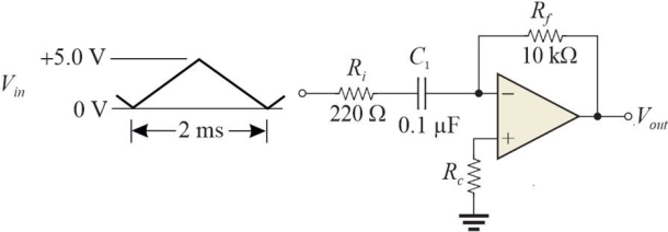 Figure 6
Refer to Figure 6. You observe large decaying oscillations on the output. A likely cause is
A)Rf is open
B)C1 is wrong value
C)Ri is a wrong value
D)VCC is open
سؤال
 Figure 5 The input is a 500 Hz, 10 Vpp square wave centered about 0 V.
Refer to Figure 5. After steady- state conditions are reached, the output will be
A)1.0 Vpp
B)2.5 Vpp
C)10 Vpp
D)5 Vpp
سؤال
 Figure 1 Assume that +Vout(max)= +13 V and -Vout(max)= -13 V
Refer to Figure 1. If the input is a 2 Vpp sine wave, the output will be
A)a ramp
B)a dc level
C)a square wave
D)an inverted sine wave
سؤال
 Figure 4 The sine wave shown is the input signal.
Refer to Figure 4. The correct output waveform is represented by
A)(a)
B)(b)
C)(c)
D)(d)
سؤال
 Figure 6
Refer to Figure 6. The output waveform is a
A)square wave
B)sine- wave
C)positive and negative triggers
D)none of the above
سؤال
سؤال
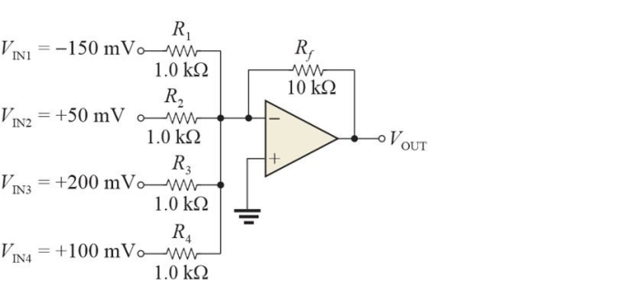 Figure 2
Refer to Figure 2. Assume there is a fault and the output = -14 Vdc. A possible cause is
A)the feedback path is open
B)a power supply connection is open
C)A and B are both possible causes
D)none of the above
سؤال
 Figure 1 Assume that +Vout(max)= +13 V and -Vout(max)= -13 V
Refer to Figure 1. If the input voltage is +11 V, the output will be
A)+11 V
B)+13 V
C)-13 V
D)-11 V
سؤال
 Figure 1 Assume that +Vout(max)= +13 V and -Vout(max)= -13 V
Refer to Figure 1. The LTP is at
A)-3 V
B)-10 V
C)+10 V
D)+3 V
سؤال
 Figure 3
Refer to Figure 3. Assume all inputs are +3.0 V. The output will be
A)-4.5 V
B)+1.5 V
C)-1.5 V
D)+4.5 V
سؤال
سؤال
سؤال
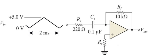 Figure 6
Refer to Figure 6. The primary purpose of Ri is to
A)attenuate the output
B)provide a path for bias current
C)avoid output drift
D)avoid noise on the output
سؤال
 Figure 5 The input is a 500 Hz, 10 Vpp square wave centered about 0 V.
Refer to Figure 5. The primary purpose of Rf is to
A)provide a path for bias current
B)prevent noise from affecting the output
C)attenuate the signal
D)avoid drift
سؤال
 Figure 5 The input is a 500 Hz, 10 Vpp square wave centered about 0 V.
Refer to Figure 5. Rc is in the circuit to balance the bias currents. A good value for Rc is
A)100 k▲
B)51 k▲
C)1.0 k▲
D)9.1 k▲
سؤال
سؤال
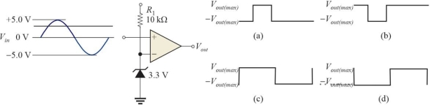 Figure 4 The sine wave shown is the input signal.
Refer to Figure 4. If the zener were reversed, the output would
A)have a longer positive output
B)be the inverse
C)have a shorter positive output
D)not change
سؤال
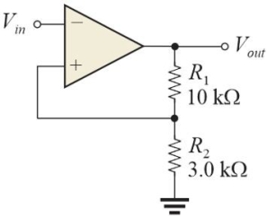 Figure 1 Assume that +Vout(max)= +13 V and -Vout(max)= -13 V
Refer to Figure 1. The UTP is at
A)+10 V
B)-3 V
C)-10 V
D)+3 V
سؤال
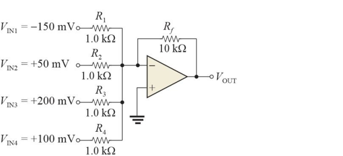 Figure 2
Refer to Figure 2. The current in Rf is
A)200 µA
B)100 µA
C)500 µA
D)1.0 mA
سؤال
سؤال
سؤال
 Figure 3
Refer to Figure 3. An open input resistor will
A)cause the output to be zero
B)appear as a 3 V input
C)cause the output to saturate
D)none of the above
سؤال
سؤال
سؤال
سؤال
سؤال
سؤال
 Figure 6
Refer to Figure 6. After steady- state conditions are reached, the output will be
A)2.5 Vpp
B)5 Vpp
C)10 Vpp
D)1.0 Vpp
سؤال
سؤال
 Figure 2
Refer to Figure 2. VOUT is
A)-2.0 V
B)+1.0 V
C)+2.0 V
D)-5.0 V
سؤال
سؤال
 Figure 5 The input is a 500 Hz, 10 Vpp square wave centered about 0 V.
Refer to Figure 5. If C1 should open, the output will be
A)a 500 Hz triangle
B)an inverted 500 Hz square wave
C)a non- inverted 500 Hz square wave
D)a dc level
سؤال
 Figure 2
Refer to Figure 2. The circuit is a
A)averaging amplifier
B)A/D converter
C)summing amplifier
D)scaling amplifier
سؤال
سؤال
 Figure 5 The input is a 500 Hz, 10 Vpp square wave centered about 0 V.
Refer to Figure 5. The output waveform is a
A)sine- wave
B)square wave with the opposite phase
C)positive and negative triggers
D)none of the above

فتح الحزمة
قم بالتسجيل لفتح البطاقات في هذه المجموعة!
Unlock Deck
Unlock Deck
1/35
العب
ملء الشاشة (f)
Deck 13: Basic Op-Amp Circuits
1
Figure 6Refer to Figure 6. You observe large decaying oscillations on the output. A likely cause is
A)Rf is open
B)C1 is wrong value
C)Ri is a wrong value
D)VCC is open
C
2
Figure 5 The input is a 500 Hz, 10 Vpp square wave centered about 0 V.Refer to Figure 5. After steady- state conditions are reached, the output will be
A)1.0 Vpp
B)2.5 Vpp
C)10 Vpp
D)5 Vpp
D
3
Figure 1 Assume that +Vout(max)= +13 V and -Vout(max)= -13 VRefer to Figure 1. If the input is a 2 Vpp sine wave, the output will be
A)a ramp
B)a dc level
C)a square wave
D)an inverted sine wave
B
4
Figure 4 The sine wave shown is the input signal.Refer to Figure 4. The correct output waveform is represented by
A)(a)
B)(b)
C)(c)
D)(d)
فتح الحزمة
افتح القفل للوصول البطاقات البالغ عددها 35 في هذه المجموعة.
فتح الحزمة
k this deck
5
Figure 6Refer to Figure 6. The output waveform is a
A)square wave
B)sine- wave
C)positive and negative triggers
D)none of the above
فتح الحزمة
افتح القفل للوصول البطاقات البالغ عددها 35 في هذه المجموعة.
فتح الحزمة
k this deck
6
The process of limiting the output of a comparator is called
A)bounding
B)clamping
C)hysteresis
D)none of the above
A)bounding
B)clamping
C)hysteresis
D)none of the above
فتح الحزمة
افتح القفل للوصول البطاقات البالغ عددها 35 في هذه المجموعة.
فتح الحزمة
k this deck
7
Figure 2Refer to Figure 2. Assume there is a fault and the output = -14 Vdc. A possible cause is
A)the feedback path is open
B)a power supply connection is open
C)A and B are both possible causes
D)none of the above
فتح الحزمة
افتح القفل للوصول البطاقات البالغ عددها 35 في هذه المجموعة.
فتح الحزمة
k this deck
8
Figure 1 Assume that +Vout(max)= +13 V and -Vout(max)= -13 VRefer to Figure 1. If the input voltage is +11 V, the output will be
A)+11 V
B)+13 V
C)-13 V
D)-11 V
فتح الحزمة
افتح القفل للوصول البطاقات البالغ عددها 35 في هذه المجموعة.
فتح الحزمة
k this deck
9
Figure 1 Assume that +Vout(max)= +13 V and -Vout(max)= -13 VRefer to Figure 1. The LTP is at
A)-3 V
B)-10 V
C)+10 V
D)+3 V
فتح الحزمة
افتح القفل للوصول البطاقات البالغ عددها 35 في هذه المجموعة.
فتح الحزمة
k this deck
10
Figure 3Refer to Figure 3. Assume all inputs are +3.0 V. The output will be
A)-4.5 V
B)+1.5 V
C)-1.5 V
D)+4.5 V
فتح الحزمة
افتح القفل للوصول البطاقات البالغ عددها 35 في هذه المجموعة.
فتح الحزمة
k this deck
11
Hysteresis avoids noise by using
A)output limiting
B)positive feedback
C)very fast comparators
D)all of the above
A)output limiting
B)positive feedback
C)very fast comparators
D)all of the above
فتح الحزمة
افتح القفل للوصول البطاقات البالغ عددها 35 في هذه المجموعة.
فتح الحزمة
k this deck
12
A simultaneous (flash)ADC is particularly useful when
A)high speed is required
B)noise rejection is required
C)there are many simultaneous input signals
D)the output must be a very large binary number
A)high speed is required
B)noise rejection is required
C)there are many simultaneous input signals
D)the output must be a very large binary number
فتح الحزمة
افتح القفل للوصول البطاقات البالغ عددها 35 في هذه المجموعة.
فتح الحزمة
k this deck
13
Figure 6Refer to Figure 6. The primary purpose of Ri is to
A)attenuate the output
B)provide a path for bias current
C)avoid output drift
D)avoid noise on the output
فتح الحزمة
افتح القفل للوصول البطاقات البالغ عددها 35 في هذه المجموعة.
فتح الحزمة
k this deck
14
Figure 5 The input is a 500 Hz, 10 Vpp square wave centered about 0 V.Refer to Figure 5. The primary purpose of Rf is to
A)provide a path for bias current
B)prevent noise from affecting the output
C)attenuate the signal
D)avoid drift
فتح الحزمة
افتح القفل للوصول البطاقات البالغ عددها 35 في هذه المجموعة.
فتح الحزمة
k this deck
15
Figure 5 The input is a 500 Hz, 10 Vpp square wave centered about 0 V.Refer to Figure 5. Rc is in the circuit to balance the bias currents. A good value for Rc is
A)100 k▲
B)51 k▲
C)1.0 k▲
D)9.1 k▲
فتح الحزمة
افتح القفل للوصول البطاقات البالغ عددها 35 في هذه المجموعة.
فتح الحزمة
k this deck
16
If a capacitor is charged with a constant current, the voltage across the capacitor is
A)constant
B)decreases
C)increases in a linear manner
D)increases in a non- linear manner
A)constant
B)decreases
C)increases in a linear manner
D)increases in a non- linear manner
فتح الحزمة
افتح القفل للوصول البطاقات البالغ عددها 35 في هذه المجموعة.
فتح الحزمة
k this deck
17
Figure 4 The sine wave shown is the input signal.Refer to Figure 4. If the zener were reversed, the output would
A)have a longer positive output
B)be the inverse
C)have a shorter positive output
D)not change
فتح الحزمة
افتح القفل للوصول البطاقات البالغ عددها 35 في هذه المجموعة.
فتح الحزمة
k this deck
18
Figure 1 Assume that +Vout(max)= +13 V and -Vout(max)= -13 VRefer to Figure 1. The UTP is at
A)+10 V
B)-3 V
C)-10 V
D)+3 V
فتح الحزمة
افتح القفل للوصول البطاقات البالغ عددها 35 في هذه المجموعة.
فتح الحزمة
k this deck
19
Figure 2Refer to Figure 2. The current in Rf is
A)200 µA
B)100 µA
C)500 µA
D)1.0 mA
فتح الحزمة
افتح القفل للوصول البطاقات البالغ عددها 35 في هذه المجموعة.
فتح الحزمة
k this deck
20
The purpose of a zener diode between the output and inverting input of a comparator is to
A)limit the output voltage
B)set the upper and lower trip points
C)limit the input voltage
D)provide a stable comparison level for the input
A)limit the output voltage
B)set the upper and lower trip points
C)limit the input voltage
D)provide a stable comparison level for the input
فتح الحزمة
افتح القفل للوصول البطاقات البالغ عددها 35 في هذه المجموعة.
فتح الحزمة
k this deck
21
A practical integrator circuit often uses an inductor in the feedback path.
فتح الحزمة
افتح القفل للوصول البطاقات البالغ عددها 35 في هذه المجموعة.
فتح الحزمة
k this deck
22
Figure 3Refer to Figure 3. An open input resistor will
A)cause the output to be zero
B)appear as a 3 V input
C)cause the output to saturate
D)none of the above
فتح الحزمة
افتح القفل للوصول البطاقات البالغ عددها 35 في هذه المجموعة.
فتح الحزمة
k this deck
23
The purpose of a priority encoder in a flash ADC is to determine
A)the sequence of binary numbers to send to the output
B)which input to encode first
C)which input has the highest value
D)the number of output bits required
A)the sequence of binary numbers to send to the output
B)which input to encode first
C)which input has the highest value
D)the number of output bits required
فتح الحزمة
افتح القفل للوصول البطاقات البالغ عددها 35 في هذه المجموعة.
فتح الحزمة
k this deck
24
An integrator circuit is useful in wave shaping applications.
فتح الحزمة
افتح القفل للوصول البطاقات البالغ عددها 35 في هذه المجموعة.
فتح الحزمة
k this deck
25
A scaling amplifier is a summing amplifier with weighted inputs.
فتح الحزمة
افتح القفل للوصول البطاقات البالغ عددها 35 في هذه المجموعة.
فتح الحزمة
k this deck
26
The output of a differentiator represents the rate of change of the input.
فتح الحزمة
افتح القفل للوصول البطاقات البالغ عددها 35 في هذه المجموعة.
فتح الحزمة
k this deck
27
The output of a comparator is normally in one of two states.
فتح الحزمة
افتح القفل للوصول البطاقات البالغ عددها 35 في هذه المجموعة.
فتح الحزمة
k this deck
28
Figure 6Refer to Figure 6. After steady- state conditions are reached, the output will be
A)2.5 Vpp
B)5 Vpp
C)10 Vpp
D)1.0 Vpp
فتح الحزمة
افتح القفل للوصول البطاقات البالغ عددها 35 في هذه المجموعة.
فتح الحزمة
k this deck
29
An R/2R ladder is generally used as an ADC.
فتح الحزمة
افتح القفل للوصول البطاقات البالغ عددها 35 في هذه المجموعة.
فتح الحزمة
k this deck
30
Figure 2Refer to Figure 2. VOUT is
A)-2.0 V
B)+1.0 V
C)+2.0 V
D)-5.0 V
فتح الحزمة
افتح القفل للوصول البطاقات البالغ عددها 35 في هذه المجموعة.
فتح الحزمة
k this deck
31
A flash ADC with a four- digit binary output requires 8 comparators.
فتح الحزمة
افتح القفل للوصول البطاقات البالغ عددها 35 في هذه المجموعة.
فتح الحزمة
k this deck
32
Figure 5 The input is a 500 Hz, 10 Vpp square wave centered about 0 V.Refer to Figure 5. If C1 should open, the output will be
A)a 500 Hz triangle
B)an inverted 500 Hz square wave
C)a non- inverted 500 Hz square wave
D)a dc level
فتح الحزمة
افتح القفل للوصول البطاقات البالغ عددها 35 في هذه المجموعة.
فتح الحزمة
k this deck
33
Figure 2Refer to Figure 2. The circuit is a
A)averaging amplifier
B)A/D converter
C)summing amplifier
D)scaling amplifier
فتح الحزمة
افتح القفل للوصول البطاقات البالغ عددها 35 في هذه المجموعة.
فتح الحزمة
k this deck
34
A differentiator circuit can output a square wave from a sine wave input.
فتح الحزمة
افتح القفل للوصول البطاقات البالغ عددها 35 في هذه المجموعة.
فتح الحزمة
k this deck
35
Figure 5 The input is a 500 Hz, 10 Vpp square wave centered about 0 V.Refer to Figure 5. The output waveform is a
A)sine- wave
B)square wave with the opposite phase
C)positive and negative triggers
D)none of the above
فتح الحزمة
افتح القفل للوصول البطاقات البالغ عددها 35 في هذه المجموعة.
فتح الحزمة
k this deck
فتح الحزمة
افتح القفل للوصول البطاقات البالغ عددها 35 في هذه المجموعة.