Deck 9: Fet Amplifiers and Switching Circuits
ملء الشاشة (f)
سؤال
سؤال
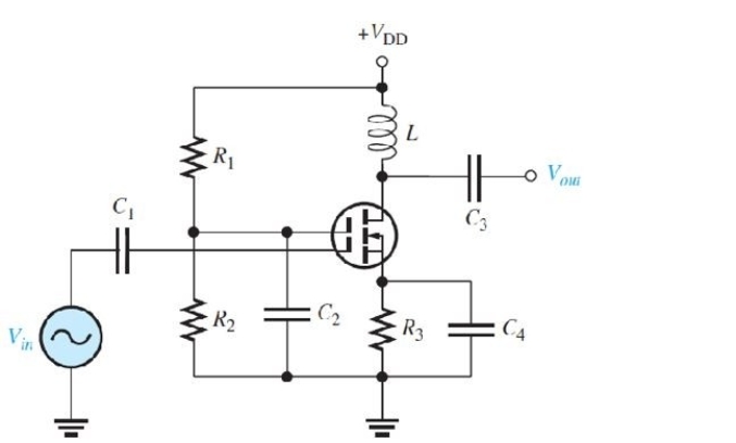 Figure 6
Refer to Figure 6. This circuit is an example of
A)an inverting amplifier
B)dual CG amplifiers
C)a cascade amplifier
D)a cascode amplifier
سؤال
سؤال
سؤال
سؤال
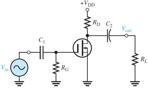 Figure 2
Refer to Figure 2. The Q- point for this amplifier is located
A)at VGS(off)
B)in the enhancement region
C)at VGS = 0 V
D)in the depletion region
سؤال
سؤال
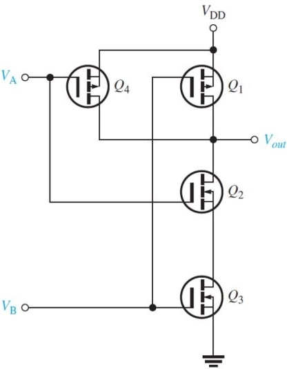 Figure 7
Refer to Figure 7. The logic circuit represented is a
A)NOR gate
B)NAND gate
C)OR gate
D)AND gate
سؤال
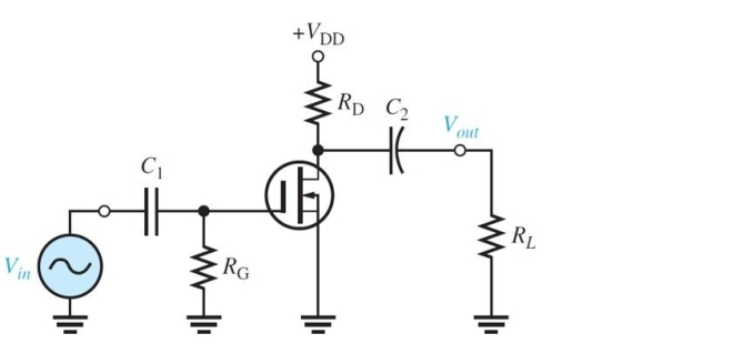 Figure 2
Refer to Figure 2. This is an example of a
A)CG amplifier
B)CC amplifier
C)CS amplifier
D)CD amplifier
سؤال
سؤال
سؤال
سؤال
سؤال
 Figure 1 The equation for gm is given in (b).
Refer to Figure 1. If C2 were to open,
A)there would be a small ac output
B)the ac load line would shift
C)both A and B
D)none of the above
سؤال
سؤال
سؤال
Figure 1 The equation for gm is given in (b).Refer to Figure 1. Assume VGS = -1 V. The expected VDS is
A)4.2 V
B)5.2 V
C)6.2 V
D)3.2 V
سؤال
 Figure 3 RS provides feedback for bias stability
Refer to Figure 3. Assume you are troubleshooting dc voltages with no signal input. You find that VDD = VD = 15 V. This could be caused by
A)open R1
B)shorted RL
C)open gate lead on the transistor
D)all of the above
سؤال
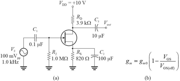 Figure 1 The equation for gm is given in (b).
Refer to Figure 1. The specification sheet indicates that gm0 is 8500 µS and VGS(off)is -2.5 V. Assume VGS = -1 V. The expected gain, Av, is
A)9.6
B)13
C)5.1
D)20
سؤال
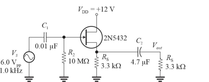 Figure 4 The spec sheet shows IGSS = 200 nA (max)at VGS = -15 V and VDS = 0 V.
Refer to Figure 4. Assume the voltage gain is 0.92. The power delivered to the load resistor is
A)1.2 mW
B)2.7 mW
C)2.3 mW
D)1.4 mW
سؤال
سؤال
سؤال
سؤال
سؤال
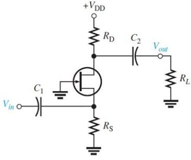 Figure 5
Refer to Figure 5. This circuit is an example of a
A)CS amplifier
B)CG amplifier
C)CC amplifier
D)CD amplifier
سؤال
سؤال
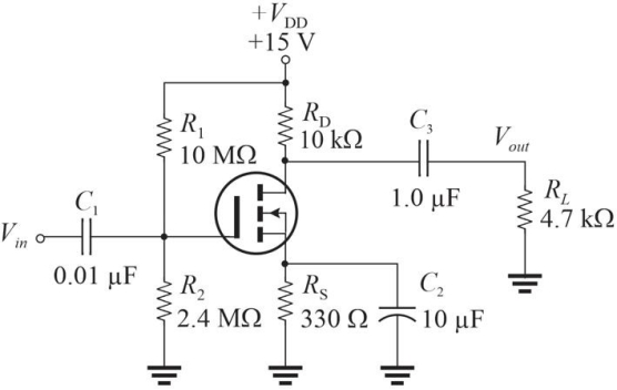 Figure 3 RS provides feedback for bias stability
Refer to Figure 3. If you are troubleshooting the ac signal and find the output is three times larger than expected and clipped. This could be caused by
A)open R1
B)open RL
C)open C2
D)shorted C2
سؤال
Figure 3 RS provides feedback for bias stabilityRefer to Figure 3. Assume that a sine wave signal is applied to the input; the output is an amplified sine wave. If gm = 15 mS, the voltage gain, AV, is
A)150
B)48
C)10
D)71
سؤال
سؤال
سؤال
 Figure 7
Refer to Figure 7. If both VA and VB are low (0), then both
A)Q1 and Q4 are off and the output is 0
B)Q1 and Q4 are on and the output is 0
C)Q1 and Q4 are off and the output is VDD
D)Q1 and Q4 are on and the output is VDD
سؤال
سؤال
 Figure 4 The spec sheet shows IGSS = 200 nA (max)at VGS = -15 V and VDS = 0 V.
Refer to Figure 4. The input resistance, RIN, assuming maximum IGSS is
A)8.1 M▲
B)75 M▲
C)8.8 M▲
D)10 M▲
سؤال
سؤال
سؤال
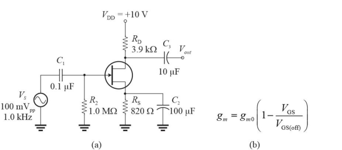 Figure 1 The equation for gm is given in (b).
Refer to Figure 1. Assume an unbypassed 36 ▲ resistor is inserted in series with RS. This primary effect of this change is to cause
A)the gain to drop
B)the output to be clipped
C)the input resistance to increase
D)a slight increase in ID

فتح الحزمة
قم بالتسجيل لفتح البطاقات في هذه المجموعة!
Unlock Deck
Unlock Deck
1/36
العب
ملء الشاشة (f)
Deck 9: Fet Amplifiers and Switching Circuits
1
Switched capacitors are used to emulate a
A)logic gate
B)relay
C)resistor
D)signal source
A)logic gate
B)relay
C)resistor
D)signal source
C
2
Figure 6Refer to Figure 6. This circuit is an example of
A)an inverting amplifier
B)dual CG amplifiers
C)a cascade amplifier
D)a cascode amplifier
D
3
Compared to a mechanical relay, a solid- state relay
A)can switch faster
B)can withstand overloads better
C)has lower on state resistance
D)all of the above
A)can switch faster
B)can withstand overloads better
C)has lower on state resistance
D)all of the above
A
4
A common- source (CS)amplifier is equivalent to a BJT
A)common- gate (CG)amplifier
B)common- base (CB)amplifier
C)common- emitter (CE)amplifier
D)common- collector (CC)amplifier
A)common- gate (CG)amplifier
B)common- base (CB)amplifier
C)common- emitter (CE)amplifier
D)common- collector (CC)amplifier
فتح الحزمة
افتح القفل للوصول البطاقات البالغ عددها 36 في هذه المجموعة.
فتح الحزمة
k this deck
5
Assume a self- biased JFET amplifier has IGSS = 10 nA, VGS = 1 V, and RG = 10 M▲. The input resistance, RIN, of the amplifier is
A)10 M▲
B)9.1 M▲
C)9.5 M▲
D)8.6 M▲
A)10 M▲
B)9.1 M▲
C)9.5 M▲
D)8.6 M▲
فتح الحزمة
افتح القفل للوصول البطاقات البالغ عددها 36 في هذه المجموعة.
فتح الحزمة
k this deck
6
Figure 2Refer to Figure 2. The Q- point for this amplifier is located
A)at VGS(off)
B)in the enhancement region
C)at VGS = 0 V
D)in the depletion region
فتح الحزمة
افتح القفل للوصول البطاقات البالغ عددها 36 في هذه المجموعة.
فتح الحزمة
k this deck
7
Compared to its BJT counterpart, A CS amplifier will typically have
A)lower input resistance
B)less distortion
C)lower gain
D)all of the above
A)lower input resistance
B)less distortion
C)lower gain
D)all of the above
فتح الحزمة
افتح القفل للوصول البطاقات البالغ عددها 36 في هذه المجموعة.
فتح الحزمة
k this deck
8
Figure 7Refer to Figure 7. The logic circuit represented is a
A)NOR gate
B)NAND gate
C)OR gate
D)AND gate
فتح الحزمة
افتح القفل للوصول البطاقات البالغ عددها 36 في هذه المجموعة.
فتح الحزمة
k this deck
9
Figure 2Refer to Figure 2. This is an example of a
A)CG amplifier
B)CC amplifier
C)CS amplifier
D)CD amplifier
فتح الحزمة
افتح القفل للوصول البطاقات البالغ عددها 36 في هذه المجموعة.
فتح الحزمة
k this deck
10
The output of a CS amplifier with a sine wave input is phase shifted by
A)180°
B)0°
C)90°
D)none of the above
A)180°
B)0°
C)90°
D)none of the above
فتح الحزمة
افتح القفل للوصول البطاقات البالغ عددها 36 في هذه المجموعة.
فتح الحزمة
k this deck
11
E- MOSFETs are excellent for logic switching because of their
A)threshold characteristic
B)lack of static sensitivity
C)negative temperature coefficient
D)all of the above
A)threshold characteristic
B)lack of static sensitivity
C)negative temperature coefficient
D)all of the above
فتح الحزمة
افتح القفل للوصول البطاقات البالغ عددها 36 في هذه المجموعة.
فتح الحزمة
k this deck
12
To minimize distortion in a CS amplifier,
A)the input resistance should very large
B)all source resistors should be bypassed
C)the signal should swing over a limited potion of the load line
D)all of the above
A)the input resistance should very large
B)all source resistors should be bypassed
C)the signal should swing over a limited potion of the load line
D)all of the above
فتح الحزمة
افتح القفل للوصول البطاقات البالغ عددها 36 في هذه المجموعة.
فتح الحزمة
k this deck
13
In order to sample a waveform that is later reconstructed, the minimum sampling rate must be equal to
A)the input frequency
B)more than four times the input frequency
C)more than ten times the input frequency
D)more than two times the input frequency
A)the input frequency
B)more than four times the input frequency
C)more than ten times the input frequency
D)more than two times the input frequency
فتح الحزمة
افتح القفل للوصول البطاقات البالغ عددها 36 في هذه المجموعة.
فتح الحزمة
k this deck
14
Figure 1 The equation for gm is given in (b).Refer to Figure 1. If C2 were to open,
A)there would be a small ac output
B)the ac load line would shift
C)both A and B
D)none of the above
فتح الحزمة
افتح القفل للوصول البطاقات البالغ عددها 36 في هذه المجموعة.
فتح الحزمة
k this deck
15
IGSS is a specification that refers to
A)gate saturation current
B)source current with the gated shorted
C)reverse leakage current
D)gate bias current
A)gate saturation current
B)source current with the gated shorted
C)reverse leakage current
D)gate bias current
فتح الحزمة
افتح القفل للوصول البطاقات البالغ عددها 36 في هذه المجموعة.
فتح الحزمة
k this deck
16
When a PWM signal is reconstructed, the purpose of the low- pass filter is to remove
A)the fundamental from the reconstructed signal
B)the modulation frequency from the reconstructed signal
C)noise from the reconstructed signal
D)harmonics from the reconstructed signal
A)the fundamental from the reconstructed signal
B)the modulation frequency from the reconstructed signal
C)noise from the reconstructed signal
D)harmonics from the reconstructed signal
فتح الحزمة
افتح القفل للوصول البطاقات البالغ عددها 36 في هذه المجموعة.
فتح الحزمة
k this deck
17
Figure 1 The equation for gm is given in (b).Refer to Figure 1. Assume VGS = -1 V. The expected VDS is
A)4.2 V
B)5.2 V
C)6.2 V
D)3.2 V
فتح الحزمة
افتح القفل للوصول البطاقات البالغ عددها 36 في هذه المجموعة.
فتح الحزمة
k this deck
18
Figure 3 RS provides feedback for bias stabilityRefer to Figure 3. Assume you are troubleshooting dc voltages with no signal input. You find that VDD = VD = 15 V. This could be caused by
A)open R1
B)shorted RL
C)open gate lead on the transistor
D)all of the above
فتح الحزمة
افتح القفل للوصول البطاقات البالغ عددها 36 في هذه المجموعة.
فتح الحزمة
k this deck
19
Figure 1 The equation for gm is given in (b).Refer to Figure 1. The specification sheet indicates that gm0 is 8500 µS and VGS(off)is -2.5 V. Assume VGS = -1 V. The expected gain, Av, is
A)9.6
B)13
C)5.1
D)20
فتح الحزمة
افتح القفل للوصول البطاقات البالغ عددها 36 في هذه المجموعة.
فتح الحزمة
k this deck
20
Figure 4 The spec sheet shows IGSS = 200 nA (max)at VGS = -15 V and VDS = 0 V.Refer to Figure 4. Assume the voltage gain is 0.92. The power delivered to the load resistor is
A)1.2 mW
B)2.7 mW
C)2.3 mW
D)1.4 mW
فتح الحزمة
افتح القفل للوصول البطاقات البالغ عددها 36 في هذه المجموعة.
فتح الحزمة
k this deck
21
In pulse width modulation, the output pulses are proportional to the
A)frequency of the input signal
B)dc level of the input signal
C)amplitude of the input signal
D)duty cycle of the input signal
A)frequency of the input signal
B)dc level of the input signal
C)amplitude of the input signal
D)duty cycle of the input signal
فتح الحزمة
افتح القفل للوصول البطاقات البالغ عددها 36 في هذه المجموعة.
فتح الحزمة
k this deck
22
To form an ac equivalent circuit for a FET amplifier, VDD is assumed to be open.
فتح الحزمة
افتح القفل للوصول البطاقات البالغ عددها 36 في هذه المجموعة.
فتح الحزمة
k this deck
23
Switched capacitors are used to emulate resistance in programmable ICS.
فتح الحزمة
افتح القفل للوصول البطاقات البالغ عددها 36 في هذه المجموعة.
فتح الحزمة
k this deck
24
A common- gate (CG)amplifier has high input resistance.
فتح الحزمة
افتح القفل للوصول البطاقات البالغ عددها 36 في هذه المجموعة.
فتح الحزمة
k this deck
25
Figure 5Refer to Figure 5. This circuit is an example of a
A)CS amplifier
B)CG amplifier
C)CC amplifier
D)CD amplifier
فتح الحزمة
افتح القفل للوصول البطاقات البالغ عددها 36 في هذه المجموعة.
فتح الحزمة
k this deck
26
A cascode amplifier is useful for higher frequencies.
فتح الحزمة
افتح القفل للوصول البطاقات البالغ عددها 36 في هذه المجموعة.
فتح الحزمة
k this deck
27
Figure 3 RS provides feedback for bias stabilityRefer to Figure 3. If you are troubleshooting the ac signal and find the output is three times larger than expected and clipped. This could be caused by
A)open R1
B)open RL
C)open C2
D)shorted C2
فتح الحزمة
افتح القفل للوصول البطاقات البالغ عددها 36 في هذه المجموعة.
فتح الحزمة
k this deck
28
Figure 3 RS provides feedback for bias stabilityRefer to Figure 3. Assume that a sine wave signal is applied to the input; the output is an amplified sine wave. If gm = 15 mS, the voltage gain, AV, is
A)150
B)48
C)10
D)71
فتح الحزمة
افتح القفل للوصول البطاقات البالغ عددها 36 في هذه المجموعة.
فتح الحزمة
k this deck
29
If a load resistor is connected to a CS amplifier the
A)the gain will increase
B)input resistance, Rin, will increase
C)both A and B
D)none of the above
A)the gain will increase
B)input resistance, Rin, will increase
C)both A and B
D)none of the above
فتح الحزمة
افتح القفل للوصول البطاقات البالغ عددها 36 في هذه المجموعة.
فتح الحزمة
k this deck
30
The output from an analog switch is pulses of different widths.
فتح الحزمة
افتح القفل للوصول البطاقات البالغ عددها 36 في هذه المجموعة.
فتح الحزمة
k this deck
31
Figure 7Refer to Figure 7. If both VA and VB are low (0), then both
A)Q1 and Q4 are off and the output is 0
B)Q1 and Q4 are on and the output is 0
C)Q1 and Q4 are off and the output is VDD
D)Q1 and Q4 are on and the output is VDD
فتح الحزمة
افتح القفل للوصول البطاقات البالغ عددها 36 في هذه المجموعة.
فتح الحزمة
k this deck
32
A common- drain (CD)amplifier is also called a source- follower.
فتح الحزمة
افتح القفل للوصول البطاقات البالغ عددها 36 في هذه المجموعة.
فتح الحزمة
k this deck
33
Figure 4 The spec sheet shows IGSS = 200 nA (max)at VGS = -15 V and VDS = 0 V.Refer to Figure 4. The input resistance, RIN, assuming maximum IGSS is
A)8.1 M▲
B)75 M▲
C)8.8 M▲
D)10 M▲
فتح الحزمة
افتح القفل للوصول البطاقات البالغ عددها 36 في هذه المجموعة.
فتح الحزمة
k this deck
34
The transconductance of a FET depends on ID.
فتح الحزمة
افتح القفل للوصول البطاقات البالغ عددها 36 في هذه المجموعة.
فتح الحزمة
k this deck
35
The gain of a common- drain (CD)amplifier is equal to gmRd.
فتح الحزمة
افتح القفل للوصول البطاقات البالغ عددها 36 في هذه المجموعة.
فتح الحزمة
k this deck
36
Figure 1 The equation for gm is given in (b).Refer to Figure 1. Assume an unbypassed 36 ▲ resistor is inserted in series with RS. This primary effect of this change is to cause
A)the gain to drop
B)the output to be clipped
C)the input resistance to increase
D)a slight increase in ID
فتح الحزمة
افتح القفل للوصول البطاقات البالغ عددها 36 في هذه المجموعة.
فتح الحزمة
k this deck
فتح الحزمة
افتح القفل للوصول البطاقات البالغ عددها 36 في هذه المجموعة.